
Ripple reduction on LNK3206 based design
Hello PI-Lupin,
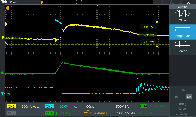
With an output inductor of 680 uH (rated at 590 mA) and 150 uH (ESR is not specified but dissipation factor is 0.16) capacitor, I am seeing a ripple of 208 mV as in the scope shot attached. With a higher capacitor of 220 uF I can see a ripple of 188-190 mV. I have tried to use a feedforward capacitor between the top feedback resistor and FB node (1uF and 0.47uF) and no changes were observed.
I also see an undershoot on the ripple waveform. This is directly inline with the Lx node waveform. How can I reduce the undershoot? With this undershoot gone, the ripple can be dropped to 96-100mV, which is very desirable. My first thoughts would be to order an extremely low ESR cap (130mOhms or lower) since I don't know what the ESR of these caps are.
Also, I plan on using this power supply with varying loads from 80mA to 250mA. How will the inductor/capacitor selection change?
Would really appreciate your help.
Files
| 첨부 파일 | 파일 크기 |
|---|---|
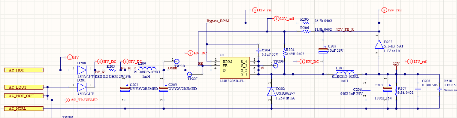
| Schematic | 167.65 KB |
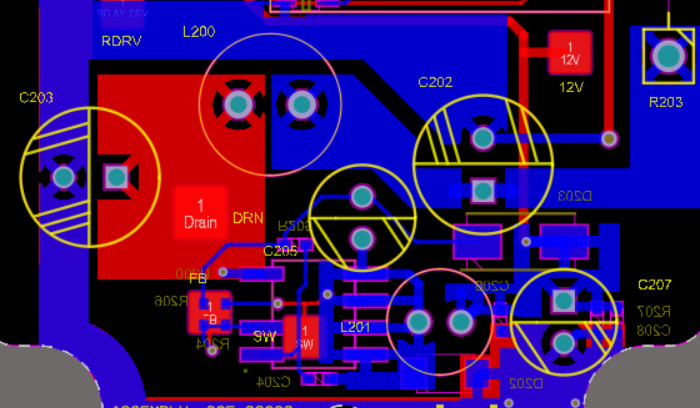
| PCB | 155.76 KB |
| Scope shot | 32.43 KB |
댓글
Hello Tommy,
Understood, I am making the appropriate changes. Can you speak to the undershoot seen in the ripple? With this current design, what are the changes required that can directly address this?
Also, that signal you are referring to is 12V_FB_R, not FB. As in, this signal does not go into the chip.
Hi saiknaram,
Thank you for clarifying that 12V_FB_R is a signal that does not go into the chip, but still it is not a good practice to route a small signal trace near/under a trace carrying a high switching current which is the DRAIN.
For the undershoot problem,
We are hoping that you are using a ripple probe for this. If not, we suggest that you use a ripple probe for probing ripple waveform, this should improves your output ripple.
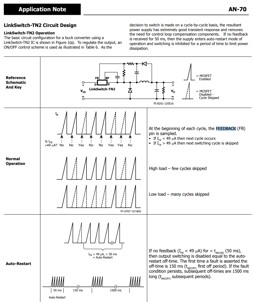
If you are using a ripple probe and the undershoot is still there, with the current design, we suggest to change your output cap to a very low ESR capacitor to reduce ripple level. The higher the ESR, the higher the voltage ripple becomes and vice versa based on the application note page 11 step 7 ESR formula an-70_linkswitch-tn2_design_guilde.pdf (power.com).
Please let me know if you need further help.
Thank you.
Understood Tommy. The second restriction of SW, Drain and input pi filter cap having a small loop sounds difficult unless you have SMD components on top and bottom layer. I am routing top for through hole and bottom for SMD.
Aso, yes, I am using a ripple probe. I was planning on using 2 68uF electrolytic caps or 2 47uF caps. Otherwise, I will look to order a low esr 100uF capacitor.
Also, it was mentioned that the SW node copper should be minimized. Does that mean hatched copper or just smaller polygon shape?
Thank you
Hello saiknaram, smaller polygon shape is preferred for the switch node copper.
If you have any questions please let me know.
Thank you.
Just wanted to confirm that we should be seeing pulses on the feedback pin just like on the switching node. I was surprised to see that at first but it looks like it's by design. I also checked the 12V_FB_R and I don't see any coupling on that signal as well. Please see the image below.
I also ended up verifying the ripple on a "fresh" board and saw lower ripple (296mV instead of 328mV for 100uF and 142mV instead of 188mV for 220uF). So with 130mOhm ESR on a 100uF capacitor or two 47uF (300mOhms each) or two 68uF (300mOhms each) capacitors in parallel should be adequate I feel. I know that going above 100uF requires a soft start capacitor in parallel with the feedback resistor as output may not reach regulation in 50ms with different loads.
Back to the undershoot on ripple, since I see it with the load plugged in, I checked that it is a peak of 520 mA or so but the inductor is rated for 590mA.
1) Can you please specify what loads are most challenging to test with? We are using a relay to connect to resistive loads, motors and inductive loads. I will be checking if 12V has excessive ripple with large inductive or resistive loads as well as up to 0.50HP motors.
2) Also, I wanted to ask you why most of the reference designs have fuses on the input rather than fusible resistors as on the 1.44W design in the TN2 datasheet? Fusible resistors have 30 seconds of reaction of time but I'm worried that the time it takes to blow the fusible resistor is too long. I'm referring to FKN200JR-73-8R2, which is a 2W 8.2 Ohm TH resistor.
![]()
| 첨부 파일 | 파일 크기 |
|---|---|
| 12_FB_R waveform.PNG | 182.01 KB |
Hello Tommy,
Could you please help to answer the above questions. Would really appreciate your earliest response on this.
Regards,
Sai
Hi Saiknaram,
Thank you for patiently waiting.
1. It will be more challenging to have an inductive compared to resistive load since resistive load has no issues because it is a heavily damped system. Due to the characteristic of inductive load to oppose any change in current, it will generate voltage that will add up to the circuit that may cause potential ringing at output.
2. You can use either fusible resistors or fuse depending on your specification and application, for example, if low no load input power is important you'll want to use a fuse instead of fusible resistor. Reference design is just a guide and it depends on your specs on how you will optimize it.
We suggest that you performed the necessary tests to ensure that the design is robust.
If you have any questions, please let me know.
Thank you.
Have a great day ahead.
Hello Tommy,
Ripple is lower now. With a 130mOhm ESR 100uF capacitor, I am getting upto 150mV of ripple. Thank you for your help!
We are planning on using this power supply with larger load at 12 V ranging from 200 mA at idle, 222 mA at wifi pairing/app use with relay and close to 400 mA at startup. We also want to this power supply for a low power at 12 V ranging from 20 mA to 90 mA. This is because it is a low power Atmel chip with a relay.
Now the problem is that I am getting loud audible noise when trying with 680 uH, 820 uH, 1 mH and 1.8 mH rated at 510 to 590 mA.
These are high pitch frequency tones in the range of 5k to 20k.
I might get a lower audible noise with the relay turned on instead of it off. But this changes with different inductor values. It happens with both 200 mA and 90 mA loads.
Why am I getting audible noise if the inductor is not saturating? Is it that the control loop is not stable?
Can you please help with this issue?
Hello saiknaram,
Good to hear that the ripple issue has been resolved.
Since it is ON-OFF control, the switching frequency gets lower as the load gets lower. That's why at light load, the switching frequency enters the audible frequency range.
To reduce the audible noise, we suggest the following:
1. Use a varnished type inductor for lower audible noise
2. Apply some rubber silicon (glue stick) or other like adhesives to secure/fixed the component(s) that causes the audible noise (inductor etc.).
If you have any concerns or question, please let me know.
Thank you.
Hello saiknaram,
Good day to you and thank you for using our product.
On your ripple waveform,
First, you can check the ESR value of the capacitor on its datasheet.
For the choosing the output capacitor and ESR value calculation, we suggest that you see page 11 step 7 of the application note an-70_linkswitch-tn2_design_guilde.pdf (power.com). Take note that the capacitor values above 100uF are not recommended as they can prevent the output voltage from reaching regulation during the 50ms period prior to auto-restart. With that, we suggest that you use a 100uF capacitor with a low/very low ESR value based on your calculation.
For your PCB layout, we see that your FB trace is directly below the DRAIN trace which is not recommended because DRAIN trace is carrying high switching current which is noisy.
With that, we suggest that you follow our recommended PCB layout consideration in page 13 of the application note an-70_linkswitch-tn2_design_guilde.pdf (power.com). You may also check "LinkSwitch-TN2 layout considerations" in pages 8-9 of this product data sheet linkswitch-tn2_family_datasheet.pdf (power.com) for additional reference.
We hope this resolves your concern. Please let me know if you need further help.
Have a great day ahead. Thank you